Growth of complex semiconductor structures
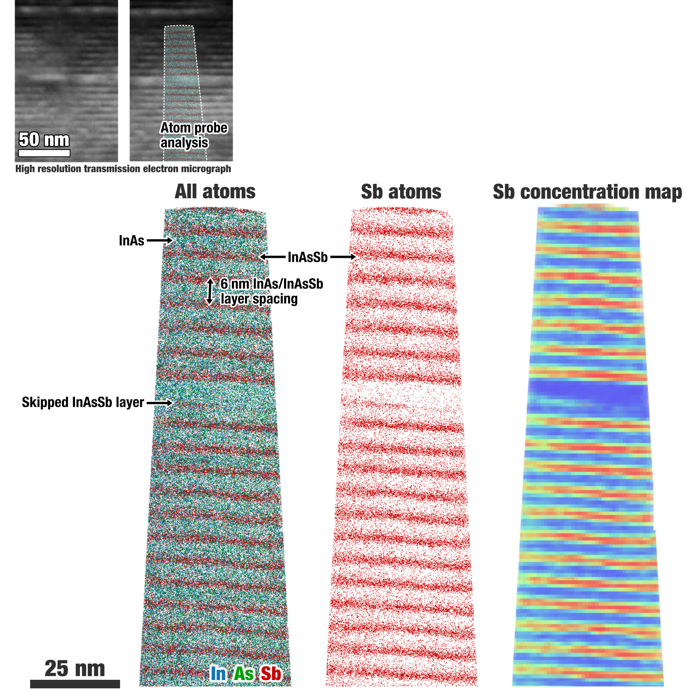
Next-generation semiconductor devices require precision growth capabilities. Here we evaluate the growth of superlattice structures comprised of alternating InAs and InAsSb layers, with particular interest on the behavior of Sb. High resolution transmission electron microscopy reveals a defective period corresponding to a "skipped" Sb-containing layer, which is also resolved by atom-probe tomography (APT). In addition, APT demonstrates that Sb also diffuses into the InAs regions, which has implications for device performance.
Related publications
- Nicole A Kotulak, Jill A Nolde, Michael B Katz, Mark E Twigg, Keith E Knipling, Dmitri Lubyshev, Joel M Fastenau, Amy W K Liu, and Edward H Aifer “Three-Dimensional Visualization of Sb Segregation in InAs/InAsSb Superlattices Using Atom Probe Tomography” J. Appl. Phys. 128 pp. 015302 (2020).